-
Mail Us Todaysales@efpcb.com
-
Company LocationShenzhen, Guangdong, China
-
+86-755-23724206Call us for more details
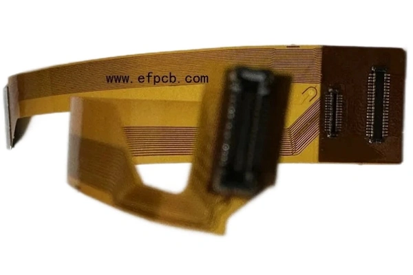
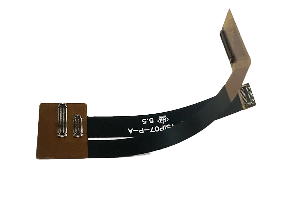
Part No.: E0215060183B
Layer count: 2 layer SAP flex PCB
Material: Polymide, 0.13mm, 1/3 OZ for all layer
Minimum trace: 2.0 mil
Minimum space (gap): 2.0 mil
Minimum hole: 0.15mm
Surface finished: immersion gold
Panel size: 75*13.5mm/1up
Application: wareable Devices
Characteristics: Flexible, 1mil Polymide, immersion gold, SAP flex PCB, flex connector for Iphone 15
In electronics, flexible printed circuit boards (FPCBs) have become increasingly popular because they are light, compact, and multi-functional. Among the different processes of fabrication, the Semi-Additive Process (SAP) is the best approach to manufacture high quality flex PCBs. Selecting a SAP Flex PCB manufacturer that can be trusted is crucial to the performance, reliability, and cost-effectiveness of your electronic designs. Here we discuss the process of building the products and key points to select best SAP flex PCB manufacturer.
The Semi-Additive Process (SAP) is a high-end PCB production technique used when producing high-density interconnects (HDI) PCBs requiring small line widths and special circuit patterns. The SAP (Semi Additive Process) method is a sophisticated process that can be used for HDI fabrication and is also suitable for other small circuits, specifically where compact structures are required. This technique allows both ultra fine traces and spaces to be manufactured, which makes it perfect for cutting edge flex PCBs utilized in Smartphones, Wearables, Medical devices, Automotive Electronics.
The following is a typical step an SAP flex PCB manufacturer will take to meet and exceed the standards of precision and performance:
1. Substrate Preparation
The process starts with a flexible material base, such as polyimide, which provides good thermal stability and flexibility. A thin layer of copper is deposited on the substrate by vacuum deposition.
2. Photoresist Application
A photosensitive resist is coated on the copper seed layer to draw the circuit pattern. This is an essential part in the production of fine lines and high density interconnections in modern electronic designs.
3. Exposure and Development
UV radiation then exposes the substrate through solder mask, the circuit pattern is transferred on the photoresist. Developer is then applied, and the undeveloped (unexposed) areas are washed away, taking with them the circuit pattern.
4. Copper Electroplating
Copper is deposited on the exposed seed layer by electroplating to form the circuit traces. That is the step that turns SAP into a viable alternative to conventional techniques by enabling control of trace width and trace thickness."
5. Etching and Cleaning
The remaining photoresist is stripped, and the copper seed layer underneath is etched to electrically isolate the trace. Then the end product is finished and cleaned to leave no residue and for best results.
6. Final Finishing
For your application, you may also be able to add other finishes, such as solder mask, gold plating, or surface treatments to improve toughness, conductivity, or corrosion protection.
An SAP flex PCB provider sells products with numerous advantages, such as:
To ensure your electronic products achieve the best performance and quality, it is important to select a trustworthy SAP flex PCB manufacturer. Here are some considerations:
Technical expertise: Seek out manufacturers that have established expertise in SAP technology and have successfully served customers for dynamic flex PCB applications.
High standard of equipment: the manufacturer should own advanced equipment as how to print fine line widths and high density patterns.
Quality assurance: The Quality Assurance certifications based on standards such as ISO 9001 and IPC solutions have proved to be an assurance of quality and reliability.
Customizable Options: A reputable/best manufacturer of your choice must have design support and customizable solution to suit your needs.
Value for money: Evaluate on the basis of price and time frame, and get the quote for the reasonable cost from the manufacturer.
Why choosing SAP for flex PCB manufacturing?
Sap enables the production of ultra-fine traces and spaces, which in turn supports high- density interconnections, increases signal integrity. That’s really important for advanced applications like smartphones, wearables, and medical devices.
Which is the best SAP flex PCB manufacturer?
Technical competence, advanced machinery, quality certification, well-established industrial reputation and robust financial status. Customizability and affordability are also things you should consider.
What SAP flex PCB materials use?
Polyimide is the most widely used substrate because of its flexibility, good thermal stability and mechanical strength. Thin copper seed layers are also necessary in the SAP process.
Which Industries Use SAP Flex PCBs?
SAP flex PCBs have found wide application in consumer electronics, the automotive industry, healthcare, aerospace, telecommunication and more.
Can multi-layer designs be used for SAP flex PCBs?
Yes, you can definitely have multi-layer PCB layout designs with SAP flex PCB providers that will help realize your complex designs and performance requirements.
The Semi-Additive Process has changed the manufacturing of flexible PCB allowing higher accuracy, density and performance. Selecting the best SAP flex PCB manufacturer is essential to take advantage of this gain and to make sure the success of your electronic products. By analyzing your manufacturer in terms of expertise on the subject matter, quality control and ability to customize products to your needs, you can request for a partner in manufacturing. With manufacturing on demand to meet the futuristic needs for useable flex PCBs SAP technology continues to lead the way in growth in the field of electronics.
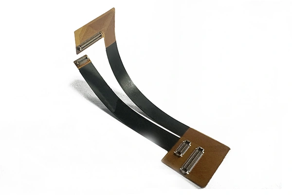
SAP flex PCB for Mobiles