-
Mail Us Todaysales@efpcb.com
-
Company LocationShenzhen, Guangdong, China
-
+86-755-23724206Call us for more details
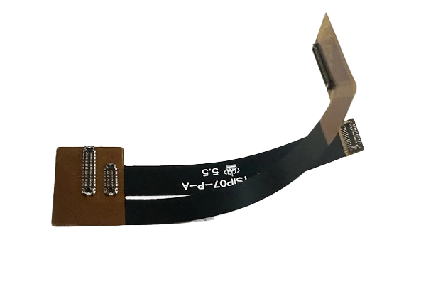
Part No.: E0215060185A
Layer count: 2 layer SAP flex PCB
Material: Polymide, 0.13mm, 1/3 OZ for all layer
Minimum trace: 2.0 mil
Minimum space (gap): 2.0 mil
Minimum hole: 0.15mm
Surface finished: immersion gold
Panel size: 75*15.5mm/1up
Characteristics: Flexible PCB connector, 1mil Polymide, immersion gold, SAP flex PCB, flex connector for Iphone 15
The rapid demand for flexible PCB connectors in contemporary electronics has enabled engineers to adapt a compact, rugged and reliable design. It's our experience as a flex PCB manufacturer, those clients who see us not as a supplier to produce their flex circuits but as part of their team, that's where things go the best. In today’s blog, we will reveal some of the manufacturer-approved tips to help you get the best performance from your designs using flexible PCB connectors, and simplify the manufacturing process.
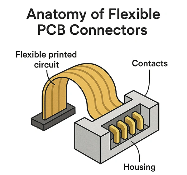
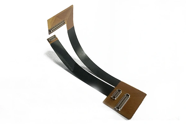
A flexible PCB connector is a dedicated flexible interconnect, such as an FPC jumper, ZIF tail, or custom flexible link, designed to electrify two or more segments of a circuit through mechanical movement. These types of connectors are vital for applications such as wearable and medical devices, automotive electronics, and aerospace systems where form factors and dynamic movement require more than a rigid connector. Flexible PCB connectors provide significant space savings over a rigid connector, durability when the flexible connector is flexed and potential cost savings as a result of reduced discrete part count. Important Issues Prior to the Design Briefing
Engaging your manufacturer early in the design process can be the single most effective cost- and time-saving step. We remember the customer who came to us late in the game after finding out the hard way that the chosen connector pitch was not manufacturable in volume. The subsequent overhaul set back their go-to-market timeline by weeks. Opening a channel early can shield you from these risks, and give up-to-the-minute insight into mechanical drawings, current load requirements, bend profiles and materials limitations.
Before you sign off on your design, think about the environment in your flexible PCB connector will operate. Does it need to flex dynamically — as a foldable wearable might — or can it stay relatively rigid? What will the temperatures and chemical exposures that it needs to endure be? We going above or beyond either of the IPC-2223 or UL standards? These factors influence everything from the ingredients used to the preoperative shaping of the connectors.
All manufacturers advise to observe at least minimum bend radius specifications to avert copper wire fatigue and ultimate failure. When bending rigid flex, it is best to bend two to four plane widths before the bend line to achieve the minimum bend radius of the flex PCB or 10D for static applications and 20D for dynamic bending. Failure to conform to this guideline undoubtedly is the master culprit for field failures. Design your connector area to tolerate slight curves rather than immediate angles and specify clearly marked areas of intended bend in your documentation.
Trace routing is also very important for the reliability of flex PCBs. Don't use sharp corners and T-junctions- these will just become stress risers during bending. 45 Expand high-stress areas with teardrop shaped pads and stagger vias placement, reduce the risk of cracking. If you are dealing with critical signal lines, be sure to consider trace width and spacing requirements for impedance control, particularly if you are working with fine-pitch flexible PCB connectors.
The choice of material affects the flexibility and lifespan of your connector. High performance uses the industry-standard polyimide, offering superior thermal stability and distinction, PET can achieve cost-effective, low-temperature fit. Trade off flexibility and durability: thinner substrate is more flexible and easier to bend, but may be less sturdy in a tape on, tape off set. Check with your manufacturer if thicker copper or dual-layer construction is appropriate for power.
All too often, however (and typically due to a designer’s lack of knowledge about manufacturing), tolerances are over-specified, adding cost and lead time. In another example, a customer eased up their tolerance stack-up and outline requirements with the help of their manufacturer, which led to 25% gains in production yield and immediate cost-savings that were evident on their balance sheet. Have faith in your manufacturer's suggested values for realistic and standard field tolerances.
The layout of a flexible PCB connector must take into consideration how the connector is assembled links and must also considerations on the way how connector are tested to validate their capacity. Connectors with polarization tabs may be advantageous for automatic assembly, while hand soldering may call for larger pads. Be sure there is always access to the electrical test points and connector orientation is well written and obviously marked to prevent miss-assembly.
Keep in mind that embedding probability in your design, can lead to: disregarding the impact of Stack-Up and stiffeners. An example of a typical error is when "designs specify a connector area but neglect to considering the stiffeners that are required. Stiffeners support the interface, however, if not used properly, they have the potential of restricting flex or causing stress concentrations. Apply them in moderation: only offer mates that are actually needed, and do not protrude into an active bend zones. Good stack up planning is of vital importance for preserving connector reliability and manufacturability.
If your design is utilizing ultra-fine pitch connectors, that’s just more reason to ensure solid impedance control and signal routing. This is extremely important for data in high-speed applications; signal integrity is everything. Work with your contract manufacturer with stack-up simulations and controlled impedance design.
“We break out the more rugged connectors, because for something like a foldable phone or a medical probe, you need a flexible PCB connector that’s going to last through thousands of flex cycles,” he explained. In recent analysis, stable circuits can remain well past 100,000 prior to structural fatigue if they are well designed and the bend radii and stress relieved coverlays are optimized. Circuit traces, score cuts, and protective coatings may be used to extend life.
In some cases, it is optional to have hard and soft parts in one design. Rigid to flex connectors combine both structural support and flexible interconnection, commonly found within either dense or multilayer constructions. Keep in mind though, that rigid-flex designs are generally more costly, and will take more planning in the form of handling layer transitions and manufacturability.
What files and what data need your manufacturer? To eliminate any issues from design to manufacturing, provide the manufacturer with comprehensive gerber files, stack-up, mechanical drawing and indicate the placement of connectors. Reference applicable IPC standard and provide a complete BOM with manufacturers for all connector parts. The best your documentation, the less chance of misunderstandings or hold ups.
Flexible PCB makes the most of collaboration early stage collaboration between designers and manufacturers is key to any success with flexible PCB connectors. Solving these types of issues using sound bend radius, trace routing and material selection best practices, while avoiding tolerance and assembly planning pitfalls, you will increase both product reliability and manufacturability. We want customers to consider their manufacturer as more than just a supplier, but as a value-added engineering partner—a partner that is with them from that initial sketch, invested in the success of the project.
Digital products