-
Mail Us Todaysales@efpcb.com
-
Company LocationShenzhen, Guangdong, China
-
+86-755-23724206Call us for more details
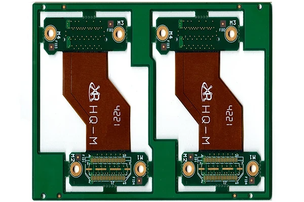
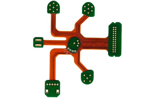
Layer account: 4 layer rigid flexible
Material: FR4 TG170 + 2mil Polymide, 1.6mm, 1 OZ for all layer
Minimum track: 4 mil
Minimum space(gap): 4 mil
Minimum hole: 0.20mm
Surface finished: ENIG
Panel size: 178*110mm/2up
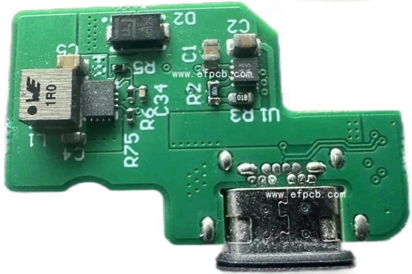
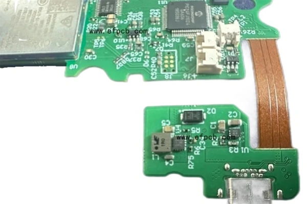
QFN chips assembly, type C assembly, high reliable PCBA, high quality PCB assembly
The continuous push for smaller electronics packages has made the Quad Flat No-lead (QFN) one of the most popular integrated circuit designs. Its small size, good thermal characteristics, and very short electrical leads make the QFN a pillar of today’s mobile devices. Yet, its distinctive leadless design also brings about different challenges that require a precise and tightly controlled process. A profitable QFN PCB assembly relies on accuracy throughout the process, from design through inspection, to guarantee solid electrical connections and reliable service.
The cornerstone of a strong solder joint is in place well before the component is dropped. It starts with good PCB layout using a well-defined central thermal pad along with peripheral landing patterns with the same dimensions as the QFN package. The application of the solder paste is potentially the most important part of the whole QFN PCB assembly procedure. A laser-cut stainless steel stencil, with thickness and aperture dimensions carefully determined, is utilized to apply a specific quantity of solder paste to the PCB pads. The quality of this print determines directly the success of the subsequent reflow soldering. Type 4 or smaller size solder powder is generally suggested to achieve the required resolution for the fine-pitch QFN dimensions.
Precise component placement and controlled reflow are the key to good IR flux reflow soldering for highest yield. Following paste inspection, typically via automated optical means, the QFN device is placed with high precision. Today’s pick & place machines have vision systems to allow the package to be aligned exactly with the footprint on the board. Placement pressure should be regulated to prevent squeezing of paste out from beneath the thermal pad which may result in bridging.
Then, the board goes through the reflow oven under a well-established thermal profile. It is designed to accomplish several objectives: to provide enough heat to raise the large thermal mass of the central pad without subjecting smaller peripheral joints to excessive heat; to activate the flux; and to allow sufficient wetting and coalescing of the solder particles. The peak temperature and time above liquidus (TAL) need to be carefully controlled to ensure that the solder joints are reliable and that the component or substrate is not thermally damaged. Thermal management is a crucial factor also in the QFN PCB assembly process.
With the imperceptible connections underneath the element, advanced technology is needed with a finished QFN PCB assembly for inspection. Alignment and visible solder bridges can be inspected using Automated Optical Inspection (AOI). But for the hidden connections under the package, there is no substitute for X-ray inspection. This inspection features a high resolution image that enables the operators to ascertain whether solder joint formation has been achieved on the peripheral leads and most importantly, to detect voiding in the solder joint on the central thermal pad. To be sure, industry standards such as IPC-A-610 have tolerances for some voiding, but too much voiding will drastically reduce thermal transfer. Lastly, the electrical test also confirms that the board is working when a fully functional and well tested QFN PCB assembly is what you want at the end of the day.