-
Mail Us Todaysales@efpcb.com
-
Company LocationShenzhen, Guangdong, China
-
+86-755-23724206Call us for more details


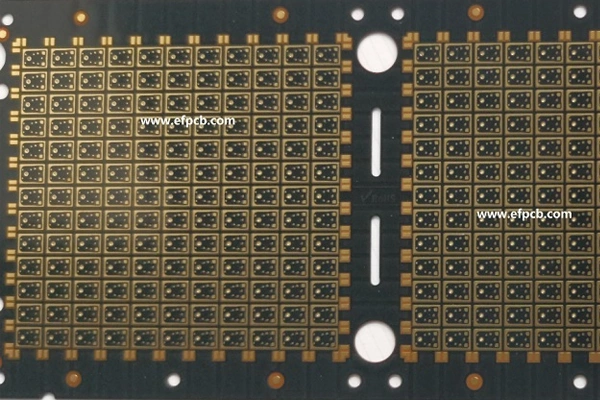
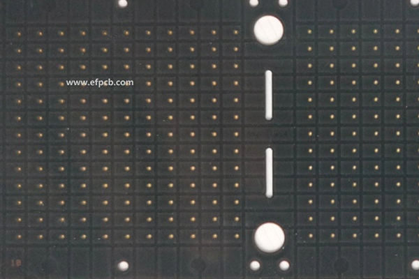
Part No.: E0207060109C
Substrate thickness: 0.2+/-0.05mm
Layer count: 2 layer
Material: SI165
Sold mask: AUS308
Minimum trace: 80 um
Minimum space: 25 um
Minimum hole: 0.15 mm
Surface finished: ENEPIG
Unit size: 3.76*2.95mm
Tired of dealing with issues associated with dependable electronic connections? Picture this: for instance, you’re happily streaming your favourite series, and then your wi-fi connection gives up on you, disturbing your marathon. l Frustrating, right? Now think what can happen in terms of connectivity issues! Tenting, ENEPIG IC substrates provide a solution herein. This enlightening blog will take us through the mysterious world of tenting and ENEPIG(Electroless Nickel Electroless Palladium Immersion Gold)IC substrates aimed at resolving your connection problems forever.
This blog is a lifesaver if they have had problems of signal interference, insufficient bonding, or component misalignment in their past projects. We’ll talk about the tenting process, showcase how ENEPIG improves electrical properties, and investigate what their top-performing applications are. In conclusion, after going through this extensive review, you will comprehend that tenting, ENEPIG IC substrate is just what you need to take care of your frustrations as far as wiring and connecting are concerned. You are now set to have secure internet experiences unlike any other once again.
It is inevitable to deny that most people, either tech fans, electrical professionals, or those that are used to their jobs being hampered by connection failures, will definitely agree with this statement. These can have a huge impact on how you use your device, ranging from signal drops and poor bonding to misaligned parts.
It’s there that tenting and ENPIG IC substrates become our savior. One way of addressing these issues is through tenting which involves covering some parts of a PCB or encapsulation. Tenting helps protect critical components and makes your connection much safer by using it as an interfering signal block.
Hence, what is ENEPIG in this regard and how does it improve the functionality of these IC substrates? PCB's electrical properties are enhanced through the application of electroless nickel electroless palladium immersion gold coating popularly referred to as ENEPIG. The latest plating technique provides superior conductance, corrosion resistant and ability to solder giving long product life and reliability under operating conditions of its application.
MEMS sensors, namely micro-electro mechanical systems, are interdisciplinary frontier research fields developed on the basis of microelectronics technology. After more than 40 years of development, it has become one of the major scientific and technological fields attracting worldwide attention. It involves electronics, machinery, materials, physics, chemistry, biology, medicine and other disciplines and technologies, and has broad application prospects. By 2010, more than 600 units around the world were engaged in the development and production of MEMS, and hundreds of products including micro-pressure sensors, acceleration sensors, micro-inkjet printheads, and digital micro-mirror displays had been developed, of which MEMS sensors accounted for a large proportion. MEMS sensor is a new type of sensor manufactured by microelectronics and micromachining technology. Compared with traditional sensors, it has the characteristics of small size, light weight, low cost, low power consumption, high reliability, suitable for mass production, easy integration and intelligent realization. At the same time, the feature size at the micron level makes it possible to complete some functions that cannot be achieved by traditional mechanical sensors.