-
Mail Us Todaysales@efpcb.com
-
Company LocationShenzhen, Guangdong, China
-
+86-755-23724206Call us for more details
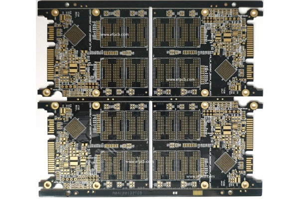
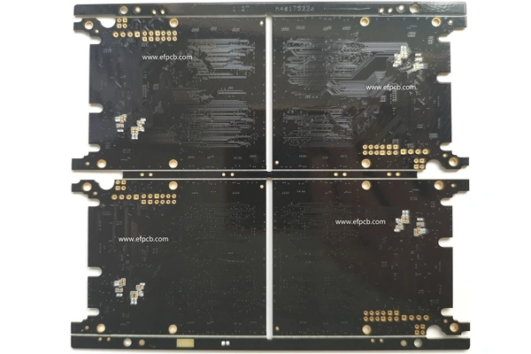
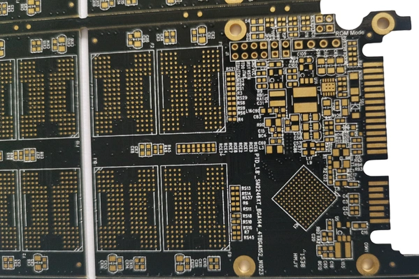
Layer count: 6 HDI PCB
Material: FR4 , 1.0 mm, High TG, 0.5 OZ for all layer
Minimum tack: 2 mil
Minimum space(gap): 2 mil
Minimum hole: 0.15mm
Surface finished: ENIG
Panel size: 220*268mm/4up
Characteristics: high density interconnect PCB, via on pad(plug with resin, copper capping), high TG, thin core 3mil thickness
High Density Interconnect (HDI) Printed Circuit Boards have transformed the electronics industry by allowing small sized high performing electronic devices. We are a leading HDI PCB manufacturer that offers advanced circuit board solutions to a wide range of industries to a high quality standard. The global HDI PCB market is expected to exceed USD 15 billion by 2026, according to a recent report from IPC, owing to an increasing number of smartphones, medical devices and automotive electronics. This article reviews the production method of HDI PCB and describes our original product.
To achieve high density circuitry along with good performance, the production of the HDI PCBs includes a series of accurate processes. The procedure starts with the selection of materials, high quality laminates such as FR4 and high performance polyimide which have very good thermal stability and electrical insulation. High Quality PCB materials are sourced from industry leading suppliers to guarantee consistency and reliable.
LD drilling is important in making HDI PCBs. In contrast to conventional mechanical drilling, the use of laser technology makes it possible to drill microvias as small as 0.1 mm in diameter. These microvias can provide a better component density and signal integrity. As a professional HDI PCB manufacturer, we apply advanced laser systems to get best via quality and position.
Sequential lamination is a must in HDI PCB process. The process itself consists of layering and bonding two or more substrates so as to create complex stack-ups with high number of conductive layers. Our patented lamination technology provides tight registration and low warp, delivering robust boards suitable for high frequency.
Our HDI PCBs are recognized for high electrical performance and the ability to miniaturize. We manufacture up to 10 layers using high end technologies such as blind vias, buried vias, via-in-pad, microvias, stack vias and sequential lamination. These features allow designers to develop small devices that do not lack in features.
As a reliable manufacturer of HDI PCB, we control the quality in every process. AOI (automated optical inspection) and X-ray testing are used to verify trace integrity and to find defects. Our products keep a low defect rate below 0.3%, which is beyond the industry standard and is satisfied by customer.
Environmental responsibility is a key part of our manufacturing ethos. We comply with the RoHS and REACH legislations; using lead-free or green materials and process. Our dedication to sustainability has made us ISO14001 and many other standards certified.
Making the right choice of HDI PCB supplier is essential to delivering electronics that are both high performance and dependable. We own the latest technology, strict quality control and environment protection, give you HDI PCBs to power your next generation of devices. With established expertise and a customer focused attitude, we are continually raising the bar in the HDI PCB industry.
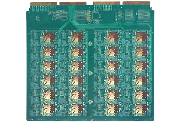
Communication Equipment Application