-
Mail Us Todaysales@efpcb.com
-
Company LocationShenzhen, Guangdong, China
-
+86-755-23724206Call us for more details
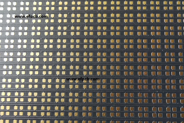
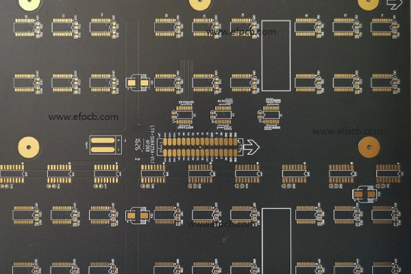
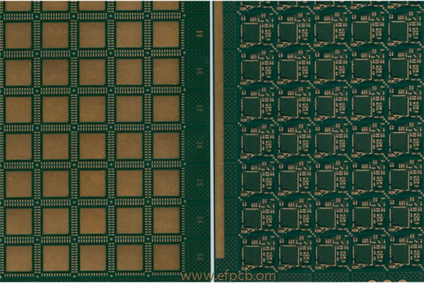
Name: VIA ON PAD PCB, HDI PCB, MULTILAYER PCB
Layer count: 6 HDI PCB
Material: FR4 , 1.2mm, TG 180, 0.5 OZ for all layer
Minimum tack: 3.6mil
Minimum space(gap): 3.6mil
Minimum hole: 0.15mm
Surface finished: ENIG
Panel size: 320*268mm/1up
Application: LED Desplay main board
Characteristics: high density interconnect PCB, via on PAD (plug with resin, and copper capping), high TG
Our one-line solutions are leading the transformation of the electronics industry with the revolutionary HDI PCBs today, High Quality PCB is looking forward to cooperate with you on the basis of mutual benefit and win-win business. Now our company is leading this revolution in small pitch LED by offering the most advanced HDI PCB solutions. These high-performance circuit boards have been developed to set the highest standards for display technology and offer phenomenal visual clarity and image quality.
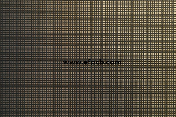
Our small pitch LED HDI PCB use pioneering manufacturing methods that establish a new bench mark in the industry. With advanced microvia technology and sequential lamination process, we can make more circuit in one unit directly help on smaller pitch. Laser drilling processes are enabled, which can be as small as 25 micrometers in diameter. Can be adapted for ever smaller components and finer pitch making this technological advancement essential.
The report states that the global demand for display application based HDI PCBs market has witnessed rapid demand growth with a rising CAGR of 12.3% for the forecast period, 2020-2028 as small pitch LED technology is getting adopted in more and more industries. Our production methodology solves the important thermal management issues in which high-density LED arrangements are subjected, utilizing the highest technology that dissipate a high level of heat and allows the product to perform in the best way for a long time.
Our unique small pitch LED HDI PCB solutions include some revolutionary features that make it different from the traditional ones. The use of any-layer via technology breaks traditional design limits, so designers can enjoy unprecedented freedom in component location and routing. This technology is especially useful for small pitch LED where space saving is essential.
We use high-quality materials at every stage and our materials have excellent dimensional stability for consistent registration accuracy from beginning to end. And this accuracy is necessary to achieve perfect concentricity in small pitch LED arrays. Our boards use specialized solder mask formulations that increase contrast and enhance the uniformity of black surfaces, allowing for substantial improvements in visual performance of led displays.
Advanced copper filling technology is turned into standard with the construction, guaranteeing solid electrical connection, and at the same time, reducing signal loss, which is very crucial to image quality in high resolution display. Our quality control is also equipped with automated optical inspection systems which can identify defects down to 10μm, ensuring that each small pitch led HDI PCB manufactured meets the highest reliability and performance standards.
With the continuous R&D investment, we have improved the process and now we can produce HDI PCB for pixel pitch less than 0.6 mm for ultra-high-resolution display with perfect visual field. Our passion for innovation and quality guarantees that customers will get the best solutions in small pitch led HDI PCB and be leaders in what is possible in display technology.