-
Mail Us Todaysales@efpcb.com
-
Company LocationShenzhen, Guangdong, China
-
+86-755-23724206Call us for more details
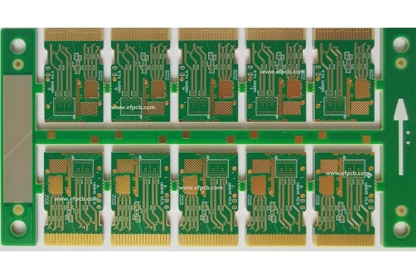


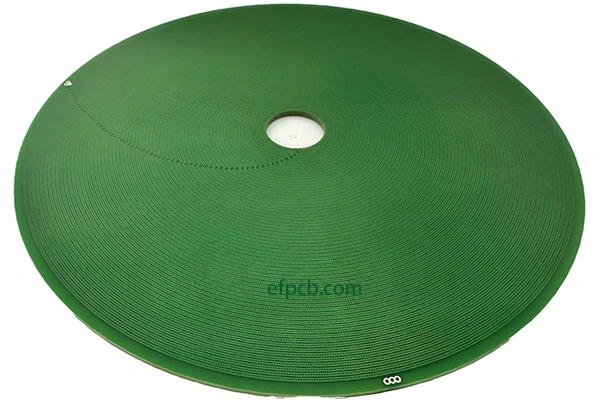
Embedded copper coin PCB, Blind and buried vias PCB
Part No.: E0617060189A
Layer count: 6 layer
Material: FR4, 1.0mm,0.5 OZ for all layer
Minimum trace: 3.8 mil
Minimum space(gap): 3.2 mil
Minimum hole: 0.20 mm
Surface finished: immersion gold +gold fingers (Au>10U")
Panel size: 128*78mm/10up
Application: Telecommunication equipment
Characteristics: Meg6 TG220, DK 3.28, immersion gold, impedance control, BGA, resin plugging, copper capping, embedded copper coin.
Evolving data centers and telecommunications networks continue to propel the need for high-speed connectivity, which has brought about innovation in transceiver technology. The 200G transceiver mainboard PCB is the foundation for these innovations, which allow for fast data transmission with little signal loss. Our company is top HDI PCB supplier to produce 200g SFP module mainboards for your demands to dimension and quality. Over the forecast period, the global optical transceiver market is anticipated to witness significant growth on account of increasing adoption of SFP modules in cloud computing and 5G infrastructure, states a recent report by MarketsandMarkets, which predicts the market to reach $9.2 billion by 2028.
When manufacturing 200G transceiver mainboard, advanced materials, precise design and comprehensive testing are needed. With the start of the process Rogers, Panasonic Megtron and other high frequency substrates are taken as the material applications which are indispensable in keeping sgnal integrity in 200G speed. As an HDI PCB manufacturer for SFP main board, our company guarantees that all the SFP main boards are strict control for super high speed data transmission.
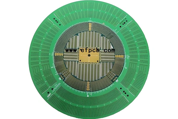
Microvia technology is the foundation for the HDI PCB fabricating for SFP modules. Laser drilling is used to form microvias that connect multiple layers without affecting signal performance. Our state-of-the-art laser technology enables us to produce via holes with diameters of down to 0.1 mm which is essential for the tight component spacing on 200G transceivers. This accuracy is important for reducing crosstalk and electromagnetic noise.
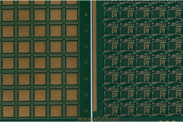
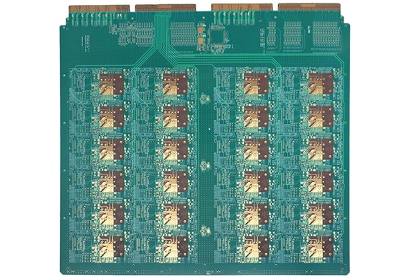
Sequential lamination adds to the stability and performance of our HDI PCB. We create high complexity stack-ups by laminating and bonding substrates meticulously layered up to 12 conductive layers. This multi-layer design includes advanced routing for SFP modules, with power management and high-speed signal routing.
Our HDI PCB solutions for SFP transceiver mainboards are known for superior electrical performance and long life. We can provide boards with fine-line traces as narrow as 40 microns, blind and buried vias, and via-in-pad layouts. These capabilities facilitate the miniaturized form factors for SFP modules while delivering strong signal integrity at 200G rates.
Quality of production is at the heart of the High Quality PCB. Each HDI PCB for SFP module will have passed through Automated Optical Inspection (AOI) and R X-ray testing to be flawless. We are proud to say that we maintain a defect rate below 0.2%, proof of our pursuit of perfection.
Environmental friendliness is also a policy of our company. All HDI PCB for SFP modules are RoHS and REACH compliant, our PCB for SFP products are made with lead free and green manufacturing process. Our plant are ISO 9001, IATF16949 and ISO 14001 accredited, we are committed to quality and environment.
Choosing a trustworthy HDI PCB manufacturer of 200G SFP transceiver mainboard is imperative to obtain stable network performance. Our company focuses on high technology, strict quality control and environment friendly, to provide the advanced HDI PCB solutions for next generation SFP modules. With proven expertise at the forefront of the industry, we enable our customers to lead in the rapidly evolving world of high-speed connectivity.