-
Mail Us Todaysales@efpcb.com
-
Company LocationShenzhen, Guangdong, China
-
+86-755-23724206Call us for more details
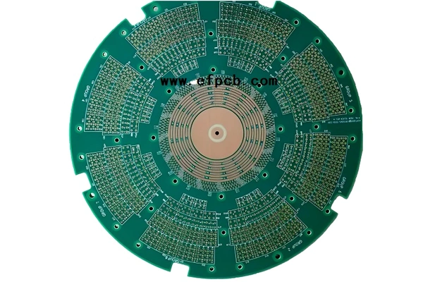
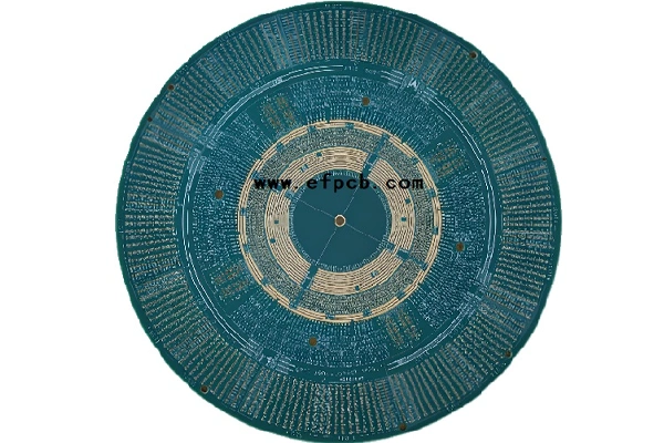
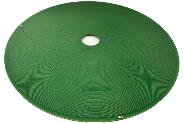
Layer count: 26 layer
Material: FR4, 3.6 mm, 1 OZ for all layer
Minimum trace: 4 mil
Minimum space: 4 mil
Minimum hole: 0.20mm
Surface finished: full board Hard Gold (Au>40U")
Panel size: 428*428mm/1up
Characteristics: High TG PCB, high multilayer PCB, hard gold PCB, IPC 6012 Class III PCB
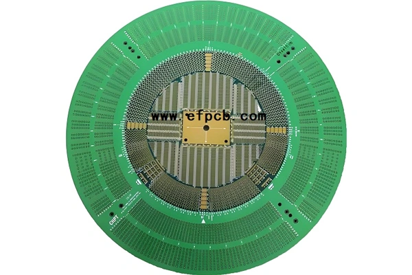
The layout varies depending on the wafer layout, I/O pitch, number of probes required, etc. Circuit designs that are complicated are created using Computer Aided Design.
Generaly need high TG, high frequency, low DK raw materials. It depends on the high frequency signals, impedance matching, etc.
To make the drills, traces, PADs, hard gold plating, ect onto PCB boards. This is usually done by a PCB manufacturer or as part of a fabrication process by an electronic manufacturing service (EMS) company.
The small probe needles of Tungsten, Nickel etc are securely fastened on the PCB terminals that come in contact with the wafer pads.
The electrical testing includes the impedance, capacitance, resistance, and signal integrity of the probe card assembly. This ensures its proper functionality before using it for real wafers testing.
Introduce the probe needles – Wider than the probe tips and serve as the stabilizing components of the system including guide plates, leveling pins, and ring.
After the completion of the fabrication of the probe card, electrical, mechanical and functional testing is conducted to fine tune the probe card and identify its characteristics before it is used in the wafer sort testing.
Some of the critical processes include lithographic fabrication of PCBs, the integration of probe needles with high precision, and testing and calibration to ensure that solid electrical contacts are made during the wafer test. Manufacturing and Assembly: Specifics of probe card manufacturing and assembly are carried out by companies specialized in the production of intricate probe cards.
The probe card is an element in semiconductor test systems. Some key points about probe cards: Some key points about probe cards:
Specific probe card design depends on the device layout, bondpad locations, and electrical test needs that are to be met. The leading manufacturers of probe cards have exposure to various technologies of devices.
In conclusion, probe cards are vital in providing an all-around test for present complex ICs in the industry before they are packaged and sold to clients. It locates at a very strategic position between the ATE system and the wafer-level devices under test.