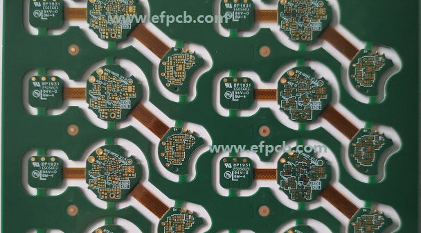
The PCB Fabrication Process in Details for Your Knowledge

Keywords: PCB Fabrication, RF PCB
The initial PCB fabrication is done with the use of two types of software. In designing the electronic schematic of the circuit to be produced there is use of Computer Aided Design (CAD) software. Computer Aided Manufacturing (CAM) software is used by engineers to produce the PCB prototype after the schematic is designed.
The first step in the fabrication process is to select the material of the printed circuit board once you design the PCB prototype. There is availability of various types of PCB materials available. The dimensions of the PCB are dictated by the design requirement.
The first process is to apply a coating of copper to the entire board after there is selection of material. By a photosensitive process the circuit layout will then be printed on the board. Then, there will be use of photo engraving process so that all the copper that is not part of the circuit layout will be etched out or removed from the board. The resulting copper will create the traces or tracks of the RF PCB circuit, two processes are used in connecting the circuit traces. To remove the unnecessary copper from the board a mechanical milling process will use CNC machines. Then, to cover the regions where traces must exist an etch-resistant, silk-screen, printing process is applied.
The PCB board contains copper traces without any circuit components at this particular point in the PCB fabrication process. Holes must be drilled at the points where the electrical and electronics parts are placed on the board so that mounting on the components can be done. With either lasers or a special kind of drill bit made of Tungsten Carbide the drilling of holes is done. Hollow rivets are inserted into them once the holes are drilled or they are even coated by an electroplating process, which helps in creating the electrical connection between the layers of the board. To coat the entire PCB with the exception of the pads and the holes a masking material is then applied. There are various types of masking material. Screen printing the board is the final step in the PCB fabrication process so labels and the legend appear at their proper locations.
- 1Understanding UL 94V-0 Flammability Rating for Printed Circuit Boards (PCBs)
- 2HDI PCB Market Outlook 2025: Future Prospects, Growth Analysis & Innovations
- 3Top 10 Flexible PCB Factories in 2025
- 4HDI PCB Design Comprehensive Guide: Mastering High Density Interconnect Technology in 2025
- 5Top HDI PCB Manufacturers (2024)
- 6IC Substrate | Comprehensive Guide (2021)
- 7PCB core raw material CCL
- 8How to Make mSAP PCB?
- 9Top 10 IC Substrate Fabricators (2024)
- 10What is IPC 4761 Type VII Via in Pad PCB?

- Skype ID: shawnwang2006
- Phone No。: +86-755-23724206
- Email: sales@efpcb.com
- Quick Contact
