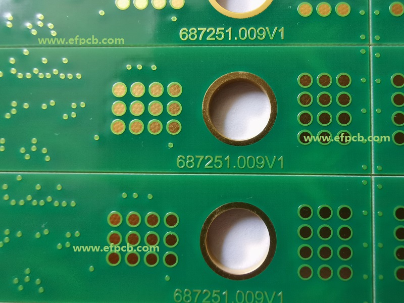
The Importance and Standard of Via on PAD Technology for PCB
Why Does PCB need Via on PAD Design

In the design of printed circuit board (PCB), Via on PAD design is a special design method, which mainly has the following functions:
1、 Meet high-density cabling requirements
Increase cabling space
With the development of miniaturization and multifunction of electronic products, the density of electronic components on PCB is getting higher and higher, and the wiring space becomes extremely limited.
The Via on PAD design can realize the electrical connection between different layers by setting vias on the pad in the limited plane space, so as to provide more path choices for wiring and effectively increase the wiring space.
For example, in the motherboard design of some high-end smart phones, due to the integration of many functional modules, the component density is very high, and the use of Via on PAD design can meet the complex wiring requirements without increasing the PCB size.
Realize complex circuit connection
In some complex circuit designs, it may be necessary to realize the connection between multiple different networks, but the traditional wiring method may not meet the requirements.
Via on PAD design can connect different networks by setting vias on key nodes to realize complex circuit functions.
For example, in high-speed digital circuits, in order to ensure the integrity of the signal, it is necessary to strictly control the impedance of the signal. Through the design of the Via on PAD, the grounding via can be introduced at a specific position to realize the reference plane switching of the signal, so as to adjust the impedance of the signal and meet the requirements of high-speed signal transmission.
2、 Improve electrical performance
Reduce signal transmission impedance
When the signal is uploaded on PCB, the discontinuity of impedance will lead to problems such as signal reflection and attenuation, which will affect the quality of the signal.
The Via on PAD design can reduce the impedance discontinuity on the signal transmission path by optimizing the position, size and shape of the through hole, so as to reduce the signal transmission impedance and improve the integrity of the signal.
For example, in high-speed differential signal transmission, by reasonably designing the position and spacing of the disk holes, the impedance of the differential pair can be more matched, the crosstalk between differential signals can be reduced, and the transmission quality of the signal can be improved.
Reduce electromagnetic interference
In electronic products, electromagnetic interference is a common problem, which will affect the normal operation of the circuit.
Via on PAD design can reduce the impact of electromagnetic interference by isolating sensitive signals from interference sources.
For example, in a PCB where analog circuits and digital circuits coexist, a Via on PAD can be set between the analog ground and digital ground to realize the division of the ground plane and reduce the interference of digital circuits to analog circuits.
3、 Improve cooling performance
Provide cooling channel
With the increasing power density of electronic components, heat dissipation has become one of the key factors affecting the reliability of electronic products.
Via on PAD design can form a heat dissipation channel on the PCB to transfer the heat from the heating element to the heat dissipation layer or external radiator to improve the heat dissipation efficiency.
For example, in the PCB design of high-power LED lighting fixtures, by setting Via on PAD on the LED pad, the heat generated by the LED can be quickly transmitted to the heat dissipation layer of the PCB, reducing the working temperature of the LED and improving its reliability and life.
Uniform heat dissipation distribution
On some large-area PCBs, if the heat dissipation is uneven, it may lead to excessive local temperature, affecting the performance and life of electronic components.
Via on PAD design can make the heat more evenly distributed on the PCB by reasonably distributing the through holes to avoid the problem of local overheating.
For example, in the design of large PCB such as server motherboard, a large number of Via on PAD are usually used to optimize the heat dissipation performance and ensure that the temperature of the whole motherboard is within a safe range.
4、 Adapt to special packaging requirements
Meet BGA and other packaging forms
Ball grid array (BGA) packaging is a common form of integrated circuit packaging, with a large number of pins and small spacing, which has high requirements for PCB design.
The Via on PAD design can provide good electrical connection and heat dissipation channel for BGA packaged chips, and meet the requirements of high density and high performance.
For example, in the design of some high-performance computer motherboards and graphics cards, BGA packaged chips are widely used, and the design of Via on PAD becomes an essential part.
Support installation of special components
In some special application scenarios, some electronic components with special shapes or sizes may need to be installed, while the traditional PCB design may not meet the requirements.
Via on PAD design can be customized according to the installation requirements of special components to provide reliable connection and fixation for special components.
For example, in some industrial control equipment, it may be necessary to install some large radiator or inductive components. By setting Via on PAD on the PCB, these components can be firmly installed and well connected.
What is Via on PAD Standard Please?
The acceptable standard for Via on PAD design mainly includes the following aspects:
1、 Electrical performance
Continuity
Via on PAD must ensure good electrical continuity. We can test the resistance value by multi meter or a special continuity tester. The resistance value must be meet our design value.
For example, for ordinary digital circuits, the on resistance of the Via on PAD should be less than 50 milliohms; For high-precision analog circuits or high-speed signal transmission lines, the on resistance is required to be lower, which may be less than 10 milliohms.
Impedance control
For high-speed digital circuits and RF circuits, the impedance of the Via on PAD shall meet the design requirements. We generally use impedance equipment to test the impedance value, to make sure Via on PAD quality under our control, the impedance value must be within the specified tolerance range
For example, for a 50 ohm transmission line, the impedance of the Via on PAD should be controlled between 45 and 55 ohms.
Signal integrity
Through the signal integrity test, the influence of Via on PAD on signal transmission is evaluated.
We can check the waveform, amplitude, rise time, fall time and other parameters of the signal by Oscillograph, network analyzer and other devices, So that ensure there is no obvious distortion, attenuation or reflection when the signal passes through the Via on PAD.
For example, for high-speed digital signals, it is required that the rise time and fall time of the signal change no more than 10% after passing through the disc hole; For RF signals, the reflection coefficient is required to be less than -15db.
2. Mechanical properties
Hole wall quality
The hole wall of the Via on PAD shall be smooth, free of cracks and burrs. The hole wall can be observed with a microscope or an electron microscope to check for defects.
The roughness of the hole wall shall meet the requirements. Generally, the roughness is required to be less than 5 μm. Rough hole wall will affect the reliability of electrical connection and may cause signal transmission problems.
Aperture accuracy
The diameter of the Via on PAD shall meet the design requirements, and the tolerance is usually within ± 0.05mm. We need to measure via diameter with X-ray or micro section devices, to ensure via diameter within specified range.
The position of the Via on PAD shall be accurate, and the deviation from the design drawing shall be within the specified tolerance range. Coordinate measuring instrument or optical detection equipment can be used to measure the position of the Via on PAD to ensure that its position accuracy meets the requirements.
For example, for high-precision PCB design, the position deviation of Via on PAD should be less than ± 0.05mm. Excessive position deviation may affect the layout of the circuit and the reliability of the electrical connection.
3. Reliability
Thermal shock test
The PCB is tested by thermal shock test to simulate the temperature change of electronic products in the actual use process. Through repeated high-temperature and low-temperature impact, check whether the Via on PAD has cracking, delamination, falling off and other phenomena.
For example, put the PCB in the temperature range of -55 ℃ to 125 ℃ for 1000 cycles of thermal shock test, and the hole in the disc should be free from any damage.
Vibration test
The PCB is tested for vibration to simulate the vibration environment of electronic products during transportation and use. We need to check if the Via on PAD was loosed or broken after applying a certain frequency and amplitude of vibration.
For example, we conduct a random vibration test with a frequency of 5-500Hz and an acceleration of 5g. The duration is 2 hours, and the Via on PAD should be free from any damage.
Weldability test
Conduct weldability test on Via on PAD to check its performance in the welding process. Immerse the PCB in the tin furnace to make the Via on PAD contact with the solder, and observe whether the solder can well wet the hole wall to form a uniform solder layer.
For example, it is required that the climbing height of solder in the Via on PAD should be at least 75% of the hole depth, and the solder surface should be smooth, free of pores, pinholes and other defects.
4. Appearance inspection
Flatness
The surface of PCB shall be flat, and there shall be no obvious bulge or depression around the Via on PAD. The flatness meter can be used to measure the surface of PCB to ensure that its flatness meets the requirements.
For example, for ordinary PCB, the surface flatness should be less than ± 0.1 mm. For high-precision PCB, the flatness is required to be higher, which may be within ± 0.05 mm.
Cleanliness
PCB should be kept clean, and there should be no residual oil, dust, welding slag and other impurities in the Via on PAD. The cleanliness of the Via on PAD can be checked by visual inspection or microscopic observation.
If there are impurities in the Via on PAD, it may affect the reliability of the electrical connection, and even cause faults such as short circuit.
Via on PAD on PCB shall be clearly identified for production and maintenance. The identification shall include hole number, network name, hole size and other information.
The identification can be carried out by means of silk screen printing, laser marking, etc., and it shall be ensured that the identification is clear, firm and not easy to wear or fall off.
5. IPC-6012D or IPC 4671 VII standard for Via on PAD,
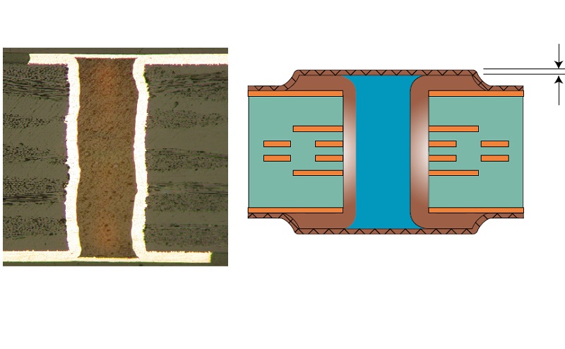
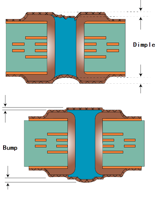
Adhesion of the metallized coating to the via fill and copper pad. Copper thickness. The planarity between the fill material and the copper surface. CTE mismatch between the fill material and metallization resulting in air gap (fill material shrinkage). Less than 100% via fill may result in a metallized cap that is too thin or a dimple that can also cause entrapped air resulting in voids in BGA solder joints. Pinholes in the metallized coatings result in non-solderable areas of a land where the capped via is intended for a BGA solder joint. Reduced solder volume is also a concern with dimples.
A: Perfect situation: without dimple or bump.
B: With dimple or bump.

|
|
Class I |
Class II |
Class III |
|
Capped copper thickness (um) |
AABUS |
5 |
12 |
|
Dimple max (um) |
AABUS |
127 |
76 |
|
Bump max (um) |
AABUS |
50 |
50 |
- 1Understanding UL 94V-0 Flammability Rating for Printed Circuit Boards (PCBs)
- 2HDI PCB Market Outlook 2025: Future Prospects, Growth Analysis & Innovations
- 3HDI PCB Design Comprehensive Guide: Mastering High Density Interconnect Technology in 2025
- 4Top 10 Flexible PCB Factories in 2025
- 5Top HDI PCB Manufacturers (2024)
- 6IC Substrate | Comprehensive Guide (2021)
- 7PCB core raw material CCL
- 8How to Make mSAP PCB?
- 9Top 10 IC Substrate Fabricators (2024)
- 10What is IPC 4761 Type VII Via in Pad PCB?

- Skype ID: shawnwang2006
- Phone No。: +86-755-23724206
- Email: sales@efpcb.com
- Quick Contact
