The Flex PCB Build Up and Fabrication Process
Keywords: Flexible PCB, Flexible PCB Manufacturer
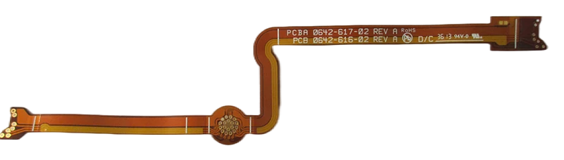
With the evolution of flexible PCB technology, latest gadgets (electronic) have advanced a lot. In the core of many delicate and sensitive electronic products, they are found.
Flex PCB Build Up
Saving the base material is the main focus, which is the primary phase. Polyimide is the primary material used for the flex circuit. This material, As compared to FR-4, is expensive and must be properly used. In the prototype PCB manufacturing, the following processes are included:
Looping: It is acceptable to add a slight amount of extra material beyond the designer's limit. a service loop is this extra material that enables the circuit assembly and servicing length.
Sizing conductor: greatest flexibility is provided by it. Particularly when you want to use the circuit for dynamic applications, you need to select the thinnest copper.
Etching: To compensate for any isotropic losses in the manufacturing process, this process is done. The line width loss is almost twice the copper foil thickness during this process. Like different types of conductors, etch masks, copper, etc, several factors impact the line width.
Routing: the conductor's routing can be easily done. Simply fold and bend, get on the perpendicular position. Reducing stress will improve bending and folding.
Ground Planes: If there is adequate electrical allocation, ground areas are created crosshatched. Improving the flexibility of the circuit from Flexible PCB Manufacturer, this aids by reducing the circuit board weight.
Flexible Printed Circuit Board (PCB) Fabrication Process
It starts with conductor width and spacing. A standard conductor width is needed by Polymer thin films. Depending on the application and design, the diameters of holes in flexible PCBs can differ.
Holes Size: The manufacturer is also capable of a flexible PCB layout and can create small holes to be well inclined.
Filleting: Filleting is a technique, where the area of the pad can be multiplied simply and the stress is divided. Filleting is needed for all the land and pads termination points on your flexible circuits. For the creation of a reliable solder joint, plated through-holes are best.
Button plating: Here, a substitute plated through-hole can be created here. To prepare through-holes and vias, manufacturers of flexible PCB use copper these days.
- 1Understanding UL 94V-0 Flammability Rating for Printed Circuit Boards (PCBs)
- 2HDI PCB Market Outlook 2025: Future Prospects, Growth Analysis & Innovations
- 3Top 10 Flexible PCB Factories in 2025
- 4HDI PCB Design Comprehensive Guide: Mastering High Density Interconnect Technology in 2025
- 5Top HDI PCB Manufacturers (2024)
- 6IC Substrate | Comprehensive Guide (2021)
- 7PCB core raw material CCL
- 8How to Make mSAP PCB?
- 9Top 10 IC Substrate Fabricators (2024)
- 10What is IPC 4761 Type VII Via in Pad PCB?

- Skype ID: shawnwang2006
- Phone No。: +86-755-23724206
- Email: sales@efpcb.com
- Quick Contact