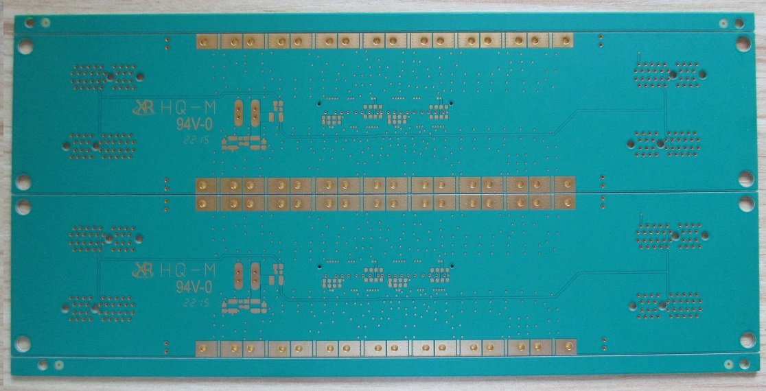
The Basics of Transmission Lines in Radio Frequency PCB

Keywords: Radio Frequency PCB
Transmission lines are structures designed to guide electromagnetic signals from one point to another with minimal distortion or loss. They are crucial in Radio Frequency PCB to maintain signal integrity, reduce reflections, and mitigate impedance mismatches that could otherwise degrade performance.
Key Concepts
- Characteristic Impedance (Z0): Characteristic impedance is a fundamental property of a transmission line, representing the ratio of voltage to current in a unit length. It determines how effectively a transmission line transfers power from a source to a load. For RF PCBs, maintaining consistent characteristic impedance throughout the trace is vital to prevent signal reflections and maintain optimal signal quality.
- Propagation Delay: The time it takes for an electromagnetic wave to travel along a transmission line from the source to the destination is called propagation delay. This becomes critical in RF PCB design, where timing is crucial for proper signal synchronization and processing.
- Reflections and VSWR: High VSWR indicates the presence of reflections due to impedance mismatches. In Radio Frequency PCB design, minimizing VSWR is essential to prevent signal degradation and maintain signal integrity.
Transmission Line Types
- Microstrip: They consist of a conductor on one side of the PCB and a ground plane on the other. Microstrip lines are relatively easy to fabricate and are suitable for designs with moderate frequencies.
- Stripline: Stripline transmission lines are sandwiched between two ground planes, providing better shielding and reduced radiation compared to microstrip lines.
- Coplanar Waveguide (CPW): CPW transmission lines feature a conductor sandwiched between two ground planes, with the signal trace exposed on the top. CPW lines offer good isolation and are suitable for RF designs that require minimal radiation.
Design Considerations for RF PCBs
- Trace Width and Spacing: The dimensions of the transmission line, such as trace width and spacing, impact its characteristic impedance. Precise control over these dimensions is crucial to maintaining the desired impedance.
- Dielectric Constant (εr): The dielectric material used in the PCB affects the propagation speed of the signal and, consequently, the characteristic impedance. Understanding the dielectric properties and their impact on the transmission line is essential.
- Signal Integrity and EMI: Proper grounding and shielding techniques are vital in Radio Frequency PCB design to mitigate electromagnetic interference (EMI) and ensure signal integrity. Careful attention must be given to grounding strategies and signal routing.


