Printing and Review of Design in the PCB Design

Keywords: Printed Circuit Board, Circuits Board
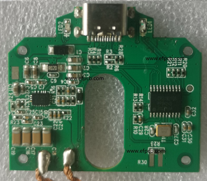
The bare board for which you provide us with the layout data and which, once we have given it to you, a PCB is what you use to mount your components, according to the industry or printed circuit board. It is more appropriately referred to as a printed wire board (PWB) or etched wiring board when the board contains just copper tracks and features and no circuit components such as capacitors, resistors, or active devices have been produced into the physical substrate of the board.
A printed circuit assembly (PCA), printed circuit board assembly (PCBA), or PCB Assembly is a PCB that has been filled with electrical components (PCBA). In colloquial use, "PCB" can refer to both bare and completed boards, depending on the context.
Engineering issues and design reviews
This is a crucial stage in the production of printed Circuits boards. It entails inspecting the design for any faults or defects, including breaches of the manufacturing standards and PCB layout rules, as well as ensuring that it adheres to the requirements.
A design review is carried out by an engineer who looks at each component of the PCB design to make sure there are no omitted parts or flawed structures. Once the design has been approved by the engineer, printing may begin.
These are some crucial inquiries for this review:
- Does the design adhere to the project's requirements as stated?
- Can the design be produced?
- Are we certain we won't make a typical design error?
PCB design printing
The PCB design is printed once all the inspections have been carried out. The PCB design is printed using a unique printer known as a plotter printer. The printer creates a film that displays the board's layers and finer details. This film is exactly like the board itself in a picture negative.
On the interior layer of the board, two ink colors are utilized during printing: clear ink to display non-conductive components like the fiberglass base and black ink to show conductive copper traces and Printed Circuit Board. On the outer layers, the same colors are used. These are lined up once the film has been produced, and a punch machine makes a registration hole through them. The registration hole is used as a guide to align the films later on in the process.
- 1Understanding UL 94V-0 Flammability Rating for Printed Circuit Boards (PCBs)
- 2Top 10 Flexible PCB Factories in 2025
- 3HDI PCB Market Outlook 2025: Future Prospects, Growth Analysis & Innovations
- 4HDI PCB Design Comprehensive Guide: Mastering High Density Interconnect Technology in 2025
- 5Top HDI PCB Manufacturers (2024)
- 6IC Substrate | Comprehensive Guide (2021)
- 7PCB core raw material CCL
- 8How to Make mSAP PCB?
- 9Top 10 IC Substrate Fabricators (2024)
- 10What is IPC 4761 Type VII Via in Pad PCB?

- Skype ID: shawnwang2006
- Phone No。: +86-755-23724206
- Email: sales@efpcb.com
- Quick Contact
