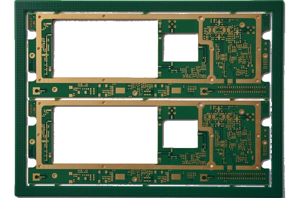
PCB Fabrication: The Digital Nervous System of Our Devices

Keywords: PCB Fabrication
PCBs are the silent enablers of our digital age. Like the human nervous system, they transmit signals, connecting various components to ensure devices function seamlessly. Just as a single neuron's role is vital to the brain's operation, so is each trace and component on a PCB. These unassuming, often green boards form the foundation of our electronic devices, ranging from smartphones and laptops to medical equipment and spacecraft. Here, you will know all about PCB Fabrication.
The Blueprint of Innovation for PCB Fabrication
The PCB fabrication process begins with a design. Engineers and designers craft a digital blueprint, specifying the layout, components, and connections of the board. This blueprint represents a fusion of art and science where creativity merges with precision to bring concepts to life. It is this design phase that defines the board's functionality, size, and even aesthetic appeal.
Material Matters
The heart of any PCB is its substrate. The choice of material, like fiberglass, polyimide, or even ceramics, plays a crucial role in the board's performance. Material properties influence factors such as heat resistance, electrical conductivity, and flexibility. Understanding these materials allows designers to tailor PCBs to the requirements of their specific applications.
Layers and Connections
Intricacy is the hallmark of PCB fabrication. Modern devices often require multiple layers of conductive traces to enable the complex interconnections between components. Fabrication facilities employ advanced techniques to create these multi-layered PCBs, with each layer contributing to the overall functionality. Copper, a highly conductive metal, is the favored choice for forming these pathways.
Etching and Assembly
The process of creating the copper traces on a PCB is a delicate dance of etching and assembly. Copper is selectively removed from the substrate using chemical etchants or a plasma etching process, leaving behind precisely defined traces. Once etching is complete, components like microchips, capacitors, and resistors are soldered onto the board. This assembly process is akin to a craftsman piecing together a complex puzzle.
Quality Assurance
Quality control is a critical stage in PCB fabrication. The boards undergo rigorous testing to ensure that every connection, every trace, and every component is in its rightful place and functioning as intended. Testing methodologies include visual inspections, automated electrical testing, and environmental stress tests to ensure reliability.
- 1Understanding UL 94V-0 Flammability Rating for Printed Circuit Boards (PCBs)
- 2Top 10 Flexible PCB Factories in 2025
- 3HDI PCB Market Outlook 2025: Future Prospects, Growth Analysis & Innovations
- 4HDI PCB Design Comprehensive Guide: Mastering High Density Interconnect Technology in 2025
- 5Top HDI PCB Manufacturers (2024)
- 6IC Substrate | Comprehensive Guide (2021)
- 7PCB core raw material CCL
- 8How to Make mSAP PCB?
- 9Top 10 IC Substrate Fabricators (2024)
- 10What is IPC 4761 Type VII Via in Pad PCB?

- Skype ID: shawnwang2006
- Phone No。: +86-755-23724206
- Email: sales@efpcb.com
- Quick Contact
