Learn About HDI Printed Circuit Boards

Keywords: HDI PCB Manufacturing
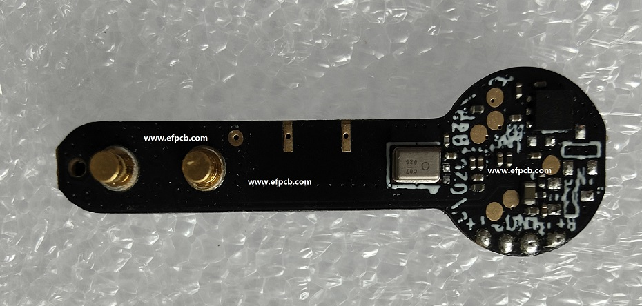
Compared to standard printed circuit boards, HDI Printed Circuit Boards are those which utilize a higher number of interconnections. In HDI PCB Manufacturing, electronics designers and developers make use of an HDI printed circuit board to be one with a pin density. The major attributes of HDI printed circuit boards are that they include denser circuit interconnections and dense component placement. It then allows for reductions in the package size or footprint of the electronic assemblies that is made from HDI printed circuit boards. In case of high-performance electronics this technology has enabled size reductions in consumer products such as mobile phones, touch screens such as used in tablet computers, laptop computers and digital cameras.
Some of the basics of HDI PCBs that includes their development, metrics, terminology and advantages is reviewed by this article.
Development of HDI Printed Circuit Board
HDI PCB Manufacturing company developed HDI printed circuit boards. It was done because there was need to provide an increased level of computational power and performance. By industries such as telecommunications this need was driven largely where the push to provide smaller and more powerful mobile phones necessitated finding a way to package more electronic circuitry in a smaller, denser package. Few of these key IC technology trends consists of:
- There are faster signal rise times
- The shrinking size of gates
- In controlling power dissipation there is reduction in operating voltage levels
- Higher levels of gate integration
- Reduction in die size
There is shifting of the trend and packaging of ICs in HDI PCB Manufacturing. It is done from the use of low-count peripheral lead frame packages towards surface mount technology. Underneath the entire surface area of the IC, it then allows the placement of interconnecting pins. Ball Grid Array (BGA) is one such technology, which in a grid pattern on the underside of the IC places the interconnecting pins. The corresponding density of pins increases as more and more pins are added to the IC packages, and there is decrease in the dimensional spacing for the circuit board traces or pads over here.
- 1Understanding UL 94V-0 Flammability Rating for Printed Circuit Boards (PCBs)
- 2Top 10 Flexible PCB Factories in 2025
- 3HDI PCB Market Outlook 2025: Future Prospects, Growth Analysis & Innovations
- 4HDI PCB Design Comprehensive Guide: Mastering High Density Interconnect Technology in 2025
- 5Top HDI PCB Manufacturers (2024)
- 6IC Substrate | Comprehensive Guide (2021)
- 7PCB core raw material CCL
- 8How to Make mSAP PCB?
- 9Top 10 IC Substrate Fabricators (2024)
- 10What is IPC 4761 Type VII Via in Pad PCB?

- Skype ID: shawnwang2006
- Phone No。: +86-755-23724206
- Email: sales@efpcb.com
- Quick Contact
