Introduction to Ceramic Circuit Board Technology
Keywords: Ceramic Substrate, Ceramic PCB
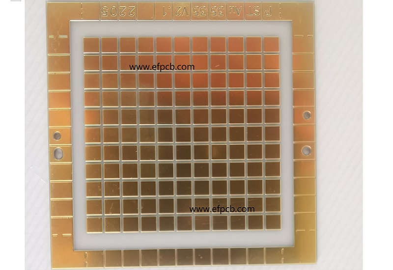
Why make circuit boards out of ceramic materials? Ceramic Substrate Ceramic PCB may be constructed in a variety of forms and are built of electronic ceramics. The most notable properties of ceramic circuit boards are their great electrical insulation and resilience to high temperatures. Low dielectric constant, low dielectric loss, high thermal conductivity, strong chemical stability, and a thermal expansion coefficient close to that of the component are all positive attributes. LAM technology, or laser rapid activation metallization technology, will be used to produce ceramic circuit boards. They are utilized in the manufacturing of LEDs, high-power semiconductor modules, semiconductor refrigerators, electronic heaters, power control circuits, hybrid power circuits, smart power components, high-frequency switching power supplies, solid-state relays, and automotive, military, aerospace, and communications electronics.
Benefits of a Ceramic PCB
Contrary to conventional FR-4, ceramic materials have superior electrical and high-frequency performance, as well as high thermal conductivity, great thermal stability, and other qualities that are lacking in organic substrates. It is a brand-new packaging material that is appropriate for the development of power electronic modules and large-scale integrated circuits.
Principal benefits:
- More conducive to heat.
- A higher thermal expansion coefficient that matches.
- Alumina ceramic circuit board with a metal film that is stronger and less resistive.
- The substrate can be soldered well, and the usage temperature is high.
- decent insulation
- The low loss at high frequencies.
- Assembly in high density is feasible.
- It has a long service life, is resistant to cosmic rays, does not include any organic materials, and has good dependability in aerospace applications.
- The copper layer may be utilized for a long time in a reducing environment since it does not have an oxide layer.
Ceramic PCB Technical Benefits
Traditional FR-4, aluminum substrate, and other substrate materials are no longer suited for the evolution of the PCB industry toward high-power and smart applications as high-power electronic devices move toward miniaturization and high speed. The conventional LTCC and DBC technologies are being gradually replaced by DPC and LAM technologies as science and technology advance. The laser technology embodied by LAM technology is more by the growth of refinement and the high-density connectivity of printed circuit boards. In the PCB business, laser drilling is now the most advanced and widely used technique. It offers excellent application value and is effective, quick, and accurate. By using laser fast activation metallization technology, rayming ceramic circuit boards are produced. The electrical qualities are good, the bonding strength between the metal layer and the ceramic is strong, and it can be repeatedly welded. The metal layer's thickness may be adjusted between 1 m and 1 mm, and the L/S resolution can go up to 20 m. direct realization of the through-hole connection enables clients to receive specialized solutions.
The ceramic circuit board has the benefits of high ceramic and metal bonding, zero shedding, blistering, etc., to produce the effect of growing together, high surface flatness, and roughness between 0.1 and 0.3 m, thanks to the laser drilling process. The diameter of a laser-drilled hole is 0.15 mm to 0.5 mm, or even 0.06 mm.
Etching
The circuit pattern is pre-plated with a lead-tin anti-corrosion layer on the copper foil that needs to be kept on the circuit board's outer layer. Then, a circuit is created by chemically etching the exposed non-conductor portion of the copper.
Etching is separated into inner and exterior layer etching depending on the various process methods. Acid etching is used for the inner layer etching, with either wet film or dry film serving as the resist. Tin lead is used as the resistance in the alkaline etching used for the outer layer.
Fundamentals of etching
Copper chloride etching with acid
Development: The portion of the dry film that has not been exposed to UV radiation is dissolved using the sodium carbonate's weak alkalinity, while the exposed portion is kept.
Etching: Use an acidic copper chloride etching solution to dissolve and remove the exposed copper surface according to a certain proportion of the solution.
Film fading: Under particular temperature and speed conditions, dissolve the protective film on the line according to a specific potion proportion.
Acidic copper chloride etching provides the advantages of simple speed control, high copper etching effectiveness, superior quality, and simple solution recycling.
Calcium etching
Film fading: To reveal the copper surface that has not been treated, use the film fading solution to fade the film on the Ceramic Substrate Ceramic PCB surface.
Etching: To remove unneeded bottom copper and leave thicker lines, use an etching solution. To encourage the oxidation reaction and stop the precipitation of cuprous ions, additives and accelerators are utilized among them. Reduced side corrosion is achieved by using the bank protection agent. The suppressor is also used to speed up the oxidation process of corroded copper and suppress the dispersion of ammonia, copper precipitation, and copper dispersion.
Fresh lotion: To remove the remaining liquid from the board, use ammonium chloride solution and ammonium monohydrate without copper ions.
Hole: Only the immersion gold procedure is appropriate for this method. Primarily eliminate surplus palladium ions from through holes that aren't coated to stop gold ions from being deposited during the gold immersion process.
Nitric acid solution is used to eliminate the tin-lead layer while melting tin.
Etching Has These Effects
- Due to gravity, the chemical liquid will create a water film on the board throughout the etching procedure, which will keep the fresh chemical liquid from making contact with the copper surface.
- Gutter Effect
- The liquid medication sticks to the lines and the spaces between the lines due to its adhesiveness. This may result in varying etching rates in open and packed locations.
- Via Effect
- As the liquid medication travels through the pores in the plate, it renews more quickly throughout the etching process, increasing the quantity of etching.
- Nozzle Swing Effect
- lines parallel to the nozzle's swing direction, as the fresh chemical liquid updates fast and easily removes the chemical liquid between the lines, causing a great quantity of etching;
- The line is perpendicular to the direction of the nozzle's swing, as the chemical liquid renewal speed is slow and the quantity of etching in Ceramic Substrate Ceramic PCB is minimal because the chemical liquid between the lines is not easily washed away by the fresh chemical liquid.
- 1Understanding UL 94V-0 Flammability Rating for Printed Circuit Boards (PCBs)
- 2Top 10 Flexible PCB Factories in 2025
- 3HDI PCB Market Outlook 2025: Future Prospects, Growth Analysis & Innovations
- 4HDI PCB Design Comprehensive Guide: Mastering High Density Interconnect Technology in 2025
- 5Top HDI PCB Manufacturers (2024)
- 6IC Substrate | Comprehensive Guide (2021)
- 7PCB core raw material CCL
- 8How to Make mSAP PCB?
- 9Top 10 IC Substrate Fabricators (2024)
- 10What is IPC 4761 Type VII Via in Pad PCB?

- Skype ID: shawnwang2006
- Phone No。: +86-755-23724206
- Email: sales@efpcb.com
- Quick Contact