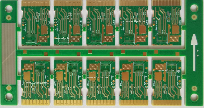
Gold Finger PCBs: The Perfect Choice for High-Performance Electronics

Keywords: Gold Finger PCB
In the realm of high-performance electronics, the importance of a reliable and efficient printed circuit board (PCB) cannot be overstated. These intricate systems, responsible for interconnecting and powering electronic components, demand precision and durability. Among the various PCB types available, one option stands out for its exceptional conductivity, corrosion resistance, and longevity - the Gold Finger PCB. In this blog, we'll explore the fascinating world of Gold Finger PCBs and discover why they are the perfect choice for demanding electronic applications.
Gold Finger PCBs, also known as gold-plated PCBs, are specialized circuit boards featuring gold-plated contact pads along their edges. These contact pads are typically used to connect the PCB to external components or connectors, such as memory modules, expansion cards, or display panels. The gold plating on these contact pads serves as a highly conductive and corrosion-resistant interface for reliable signal transmission.
One of the primary advantages of Gold Finger PCBs is their exceptional conductivity. Gold is an excellent conductor of electricity, outperforming other commonly used metals like copper or silver. The low electrical resistance of gold ensures minimal signal loss and efficient transmission of data, making it ideal for high-frequency applications and complex circuitry.
Moreover, gold is highly resistant to corrosion, oxidation, and tarnishing, which can compromise the integrity of electrical contacts. The protective gold plating on the contact pads of Gold Finger PCBs ensures long-lasting performance, even under harsh environmental conditions or in high-humidity environments. This reliability is crucial for mission-critical electronics found in aerospace, medical, and industrial applications.
Another notable advantage of Gold Finger PCB is its superior durability. The gold plating acts as a protective layer, shielding the underlying copper traces from wear, tear, and exposure to external elements. This increased durability ensures that the PCB remains in optimal condition for extended periods, reducing the risk of electrical failures or intermittent connections.
Furthermore, gold is a highly malleable metal, allowing it to withstand repeated insertions and removals without significant wear. This property is particularly beneficial in applications requiring frequent board-to-board connections or hot-swapping components, such as servers, high-end graphics cards, or telecommunications equipment.
Gold Finger PCB offers a multitude of benefits that make them a preferred choice for high-performance electronics. From their superior conductivity and reliability to enhanced durability, these specialized circuit boards provide a robust and long-lasting solution for demanding.


