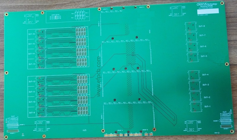
Difficulties in Fabrication of Backplane PCBs

Keywords; Backplane Board, Backplane PCB
Connected and placed on one PCB, a Backplane PCB is a collection of multiple connectors generally. Carrying signals like a cable from one connector to another is its responsibility by nature but enough good health such as power supply rails, return paths, differential paired signals, and single-ended are present. Over a backplane PCB, The PCBs with semiconductor ICs are directly press-fit. Daughter cards are these PCBs or insertable cards. On the required pins of destination connectors, it makes the pins of source connectors to be exactly connected.
To a motherboard PCB, A backplane PCB is somehow similar in complexity in respect of parameters of PCB design but in functionality and manufacturing process, it has many differences. With high pin cunt semiconductor ICs, A motherboard is well known to be a densely routed signals board. On the back of boards, a backplane is considered enough connectivity board on the other end. But, as compared to a connectivity board, a Backplane Board is much more used especially for high data rate communication systems. In between daughter boards, a backplane PCB transports all electrical connectivity of powers and signals. Being extracted or press-fit, it also supports and holds daughter cards over it.
The manufacturing effort and cost of increased design increase the throughput of the system. Wire-wrapped sockets and connectors are present in the early times' backplanes. Using advanced manufacturing skills and PCBs materials for backplane PCBs is being realized by data speed in newer systems. Along with the existing ones, it originated further PCB manufacturing constraints. Over wire-wrapped backplanes, PC (Printed Circuit) based Backplanes are preferred due to their data carriage capability and increased reliability. Semiconductor chips are not present in Backplanes In common practice. However, they contain small electronic parts like chassis, capacitors, resistors, and filters ground circuitry over them.
Two major Difficulties of Backplane Manufacturing
High-density etching
Their mounting pads and holes use a significant part of PCB real-estate due to the high count of connectors in a backplane PCB. Instead of an increasing number of layers, the PCB designers strive to increase signal routing density maintaining trace length and impedance. Etching complexity is increased by the increased signals density.
PCB Pressing
Drilling becomes more complicated in thicker backplane manufacturing. Multiple times hole drilling is needed by a lengthy drill. It decreases the Backplane PCB yield and drilling accuracy percentage. High-frequency performance gets degraded.
- 1Understanding UL 94V-0 Flammability Rating for Printed Circuit Boards (PCBs)
- 2HDI PCB Market Outlook 2025: Future Prospects, Growth Analysis & Innovations
- 3Top 10 Flexible PCB Factories in 2025
- 4HDI PCB Design Comprehensive Guide: Mastering High Density Interconnect Technology in 2025
- 5Top HDI PCB Manufacturers (2024)
- 6IC Substrate | Comprehensive Guide (2021)
- 7PCB core raw material CCL
- 8How to Make mSAP PCB?
- 9Top 10 IC Substrate Fabricators (2024)
- 10What is IPC 4761 Type VII Via in Pad PCB?

- Skype ID: shawnwang2006
- Phone No。: +86-755-23724206
- Email: sales@efpcb.com
- Quick Contact
