A Detailed Introduction to Ceramic PCB
Keywords: Ceramic Substrate Ceramic PCB
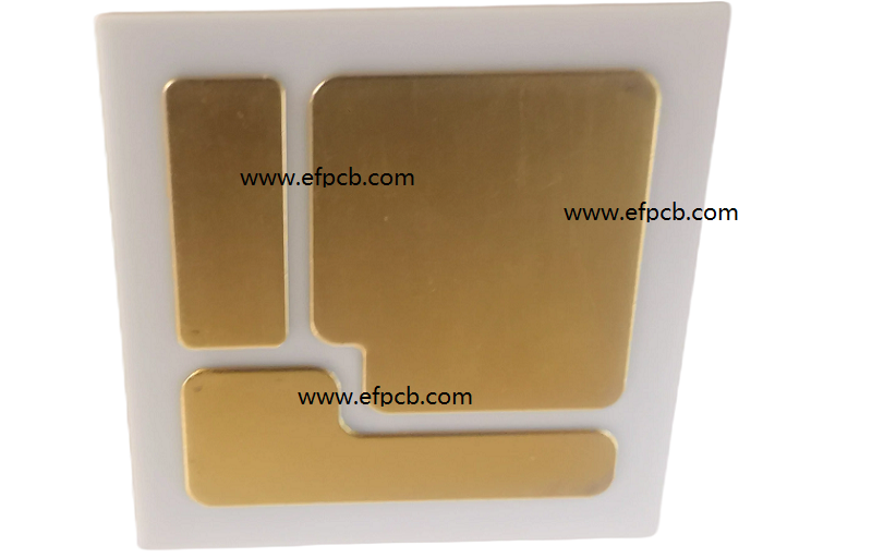
A ceramic PCB is a unique type of process board in which, at high temperatures, copper foil is directly bonded to the single- or double-sided ceramic substrate surface made of alumina (Al2O3), aluminum nitride (AlN), beryllium oxide (BeO), or silicon carbide (SiC). In addition to having superior electrical and high-frequency performance than metal core PCBs by a factor of 10 to 100, ceramic PCBs also have better heat transfer characteristics. Its expansion coefficient is likewise small (CTE). The greatest qualities of both FR4 and metal-core PCBs are said to be found in ceramic PCBs.
A printed circuit board that uses ceramics as the substrate, such as silicon nitride, aluminum oxide, and aluminum nitride, is known as a ceramic PCB. Magnetron sputtering is used to adhere the conductive layers of the ceramic PCB to the ceramic substrate. For the spotlight, a ceramic PCB is built with LEDs as shown below.
Ceramic PCB Described
Ceramic PCBs are produced at substantially greater temperatures than regular PCBs since they are made primarily of ceramics. Ceramics used for PCBs have the benefits of both metal and FR4 as PCB base materials. Aluminum and copper have great thermal conductivity but are conductors, in contrast to FR4 materials, which are electrically insulating but have low thermal conductivity. Since ceramics are effective insulators, ceramic PCBs do not need an electrical insulation layer and have high thermal conductivity.
Ceramic PCBs are transformed into ceramic PCBAs when they are mounted with LED chips, ICs, and other components. LEDs may be put together on ceramic PCBs using the flip-chip or wire bonding techniques. In high-power and high-frequency applications including car-scale power controllers, variable optical systems, exchange converters, solar power batteries, and high-current LED lights, ceramic PCBAs are frequently the key components.
What Is The Structure Of A Ceramic PCB?
A ceramic substrate layer, a copper layer, and a solder mask layer make up a single-layer ceramic PCB. To assist you to comprehend what a ceramic PCB is, we shall discuss the structure of double-layer ceramic PCBs.
The construction of a single-sided, double-layer ceramic PCB made using the standard lamination technique is shown below.
Ceramic substrate: Unlike aluminum or FR4, ceramic provides superior electrical insulation as well as thermal conductivity. Ceramic substrate, therefore, serves two purposes: heat dissipation and insulation between circuit layers. PCB holes are required for double-layer and multilayer ceramic PCBs, and the vias are drilled by laser in the ceramic substrate. After that, copper plating is used to fill the PCB vias.
Copper coating: A thin copper foil serves as a copper layer. With the aid of magnetron sputtering, it adheres to the ceramic substrate. The circuit is etched onto the copper foil using the photoresist layer of the yellow light technique after the copper foil has adhered to the ceramic substrate.
The dielectric layer (PP): PP may be composed of phenolic resin, epoxy resin, unique thermal conductive elements, etc. The two nearby ceramic substrate boards are joined together via the dielectric layer. The total thermal conductivity of the ceramic PCB is decreased by PP, which has a lower thermal conductivity than ceramics. So, for situations where there are less stringent criteria for heat dissipation, a ceramic PCB with a dielectric layer is employed.
Solder mask: Copper wires that are exposed are shielded from solder, metals, and environmental deterioration by solder masks. After the PCB is laminated, a solder mask is put above the circuit layer. The solder mask can be any color, including green, white, beige, etc. Because of its superior performance and ceramic PCB materials, a ceramic PCB is special.
In comparison to conventional PCBs, ceramic PCBs are stronger mechanically, have less war page, are more resistant to thermal shock, have a lower DK/Df, are more thermally conductive, have a closer thermal expansion coefficient with silicon, are more chemically stable, and do not absorb water.
A ceramic PCB may be three-dimensional and serve as a support component for modules in addition to transporting components.
Ceramic PCB types
Ceramic PCBs are categorized by the classification of ceramic substrates as follows:
The most popular type of ceramic PCB is made of alumina (Al2O3). Also, the least expensive ceramic PCB substrate is aluminum oxide.
Aluminum nitride PCBs (AlN): More costly than alumina PCBs, aluminum nitride PCBs are also often utilized in ceramic PCBs. AlN outperforms alumina in terms of high-frequency performance and thermal conductivity.
PCBs made of silicon nitride (Si3N4): Si3N4 is more expensive than AlN. IGBT modules, car-scale modules, and military/aerospace/aviation modules are only a few examples of power electronic modules that employ silicon nitride PCBs because of their great mechanical strength and durability.
PCBs made of silicon carbide (SiC): diamond is silicon carbide. High thermal conductivity is present. SiC also has a high conductivity as an electrical semiconductor. Laser fields are where silicon carbide PCBs are mostly employed.
made of boron oxide (BeO): BeO is toxic yet has a thermal conductivity a dozen times greater than alumina. BeO PCBs are employed in high-frequency and high-power applications because of their low DK and Df.
Ceramic PCBs can be categorized in one of the following ways according to their manufacturing processes:
HTCC ceramic PCBs: HTCC, short for high-temperature co-fired ceramic, is the oldest process for producing ceramic PCBs. High-power applications can use HTCC ceramic PCBs, but not high-frequency or high-speed ones.
Ceramic PCBs using direct bonding copper (abbreviated DBC): DBC requires lower temperatures than HTCC. PTH vias are absent from DBC ceramic PCBs. They are primarily employed as packaging for LED gadgets, power electronic modules, etc.
PCBs made of thick film ceramic: thick film ceramic PCBs need a minimum circuit line spacing of 60 mm. However, the thick film ceramic PCB's circuit is extremely precise. They are primarily utilized in applications with modest power needs.
Low-temperature co-fired ceramic, or LTCC ceramic PCBs, are what they are called. Three-dimensional and multilayer LTCC ceramic PCBs are typical. Particularly suited for high-frequency communication devices are LTCC ceramic PCBs.
PCBs made on thin-film ceramic are highly precise in their circuitry. The circuit layer's copper thickness, however, has a limit. Thin-film ceramic PCBs are appropriate for small-sized electronics and high-precision packaging.
DPC ceramic PCBs are a development of thin-film technology; DPC stands for direct plating copper. DPC ceramic PCBs can feature highly precise circuitry and can be three-dimensional. High-power and high-frequency applications employ them.
The three-dimensional architecture of the ceramic PCB enables them to sustain modules mechanically in addition to loading and connecting parts for high-power devices and packaging.
- 1Understanding UL 94V-0 Flammability Rating for Printed Circuit Boards (PCBs)
- 2HDI PCB Market Outlook 2025: Future Prospects, Growth Analysis & Innovations
- 3Top 10 Flexible PCB Factories in 2025
- 4HDI PCB Design Comprehensive Guide: Mastering High Density Interconnect Technology in 2025
- 5Top HDI PCB Manufacturers (2024)
- 6IC Substrate | Comprehensive Guide (2021)
- 7PCB core raw material CCL
- 8How to Make mSAP PCB?
- 9Top 10 IC Substrate Fabricators (2024)
- 10What is IPC 4761 Type VII Via in Pad PCB?

- Skype ID: shawnwang2006
- Phone No。: +86-755-23724206
- Email: sales@efpcb.com
- Quick Contact