A Detailed Guide on The IC Substrate Technology
Keywords: IC Substrates
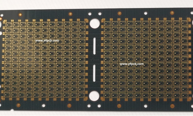
A vital unique fundamental material in advanced packaging, IC Substrates is utilized to package bare IC (integrated circuit) chips. It is also referred to as IC package substrate. With a conductive network of wires and holes, the IC substrate serves as the link between the IC chip and PCB.
Via a conductive network of traces and holes, IC substrates act as the link between the IC chip(s) and the PCB. IC substrates are equipped with vital features including signal and power delivery, heat dissipation, and circuit support and protection.
The PCB industry's greatest level of downsizing, IC substrates have several features in common with the production of semiconductors. Using wire bonding or flip-chip techniques, IC chips are bonded to a variety of IC substrates made by Rocket PCB.
BGA (ball grid array), CSP (chip level package), and other new integrated circuits (ICs) have developed quickly, necessitating the creation of novel packaging substrate. The popularity and use of IC substrate PCB, along with any layer of HDI PCB and flexible rigid PCB, has skyrocketed as one of the most sophisticated PCBs (printed circuit boards). It is now commonly utilized in electronic updating and telecom.
The development of IC substrate
Conventional integrated circuit (IC) packaging employs a lead frame as the substrate of the IC conduction line and supporting IC, connecting pins on either side or all the way around the lead frame, such as in two-sided pin flat packages, four side pin flat packages, and so forth. Since there aren't too many pins, this packing technique can also satisfy the specifications. The typical size of an IC is decreasing and the degree of integration is increasing with the advancement of semiconductor technology. The matching IC package is moving in the direction of ultra-narrow pitch, ultra-miniaturization, and ultra-multi-pin. The conventional lead bundle has fallen short of the standards.
Substrate classification for ICs
As already noted, there are several methods to categorize packaging substrates, chiefly according to the packing technique, the material characteristics, and the application sectors.
1. In line with packing procedures
Wire bonding packaging substrate and flip-chip packaging substrate are two categories of packaging substrate.
1.1 Grouping based on bonding technology
- Wire fusion
- FC bonding
- TAB
1.2 Substrat for flip-chip packing
- BGA IC substrate: The IC substrate has good electrical and heat dissipation performance and has a large increase in chip pin density. As a result, it works with IC packages that have more than 300 pins.
- CSP IC substrate: CSP is a single chip package that is lightweight, compact, and of an IC-like size. The principal applications for CSP IC substrate are electronic items with few pins, communications equipment, and memory products.
- FC IC substrate: FC (flip chip) is a flip-chip package with high performance, efficient heat dissipation, low circuit loss, and low signal interference.
- MCM IC substrate: A multi-chip module is referred to as an MCM IC Substrates. This kind of IC substrate incorporates various-function chips into a package. The product may thus be the best option as a result of its characteristics, which include lightness, thinness, shortness, and miniaturization. This sort of substrate obviously performs poorly in signal interference, heat dissipation, precise wiring, and other areas since several chips are placed in a single package.
2. Based on various substrate materials
The three types of packaging substrate are rigid board, flexible board, and ceramic substrate.
- Substrate for rigid ICs: Epoxy resin, BT resin, or ABF resin are the primary materials. Around 13 to 17 ppm/°C is its CTE (coefficient of thermal expansion).
- Flex IC substrate: It has a CTE of 13 to 27 ppm/°C and is mostly comprised of PI or PE resin.
- Ceramic IC substrate: This type of substrate is mostly constructed of ceramic materials like silicon carbide, aluminum nitride, or alumina. It has a CTE that is rather modest, between 6 and 8 ppm/°C.
3. Depending on various application fields
Memory chip packaging substrates, MEMS packaging substrates, RF module packaging substrates, processor chip packaging substrates, and high-speed communication packaging substrates are some of the subcategories of packaging substrates that can be found in mobile intelligent terminals, services/storage, etc.
IC substrate manufacturing technology
We must first comprehend the three different PCB manufacturing methods. There are now three different types of manufacturing procedures for PCB and IC substrates: subtractive process (SP), additive process (AP), and modified semi-additive process (MSAP).
1. Subtraction technique (SP): This is the most common method for producing PCBs. It involves first plating a copper layer of a certain thickness on a copper-clad laminate, applying a dry film to shield the circuit and through-holes, and then etching away any extra copper sheet. The main issue with this procedure is that the copper layer's side will also be etched during the etching process. Only standard PCB, FPC, and HDI PCB products can use PCB since the minimum line width/spacing of PCB must be more than 50 m (2 mil) due to the presence of lateral etching.
2. The addition technique (AP): The addition technique (AP) involves first exposing the circuit to an insulating substrate containing a photosensitive catalyst, followed by selective chemical copper deposition on the thick circuit that has been exposed to create a finished PCB. As this process does not need lateral etching, it can fabricate parts with very high accuracy—less than 20 m. This method is now utilized to make WB or FC IC substrate, and its method can get 12 M / 12 M. However, it has high substrate and process flow requirements, high costs, and low output.
3. Modified semi-additive process (MSAP): First, a thin copper layer is electroplated on a copper-clad laminate. Next, the areas that do not need to be electroplated are protected. Finally, the copper layer is electroplated once more and coated with an anti-corrosion coating. Finally, the more chemical copper layer is removed by flash etching, leaving the necessary copper layer line. The duration of flash corrosion is relatively brief at the beginning of electroplating because the copper coating is so thin, therefore side corrosion has less of an impact.
The MSAP process, which is the most popular way to manufacture fine circuit boards, offers the benefits of high yield and cheap production cost when compared to the subtraction technique and addition method. The production of CSP, WB, and FC IC Substrates as well as other fine line substrate boards makes extensive use of this technology. While the SLP (substrate-like PCB) is a type of printed circuit board, its minimum line width and line spacing are 30 mm and 30 mm, respectively. As a result, it cannot be created using the subtraction approach and requires MSAP process technology.
- 1Understanding UL 94V-0 Flammability Rating for Printed Circuit Boards (PCBs)
- 2HDI PCB Market Outlook 2025: Future Prospects, Growth Analysis & Innovations
- 3HDI PCB Design Comprehensive Guide: Mastering High Density Interconnect Technology in 2025
- 4Top 10 Flexible PCB Factories in 2025
- 5Top HDI PCB Manufacturers (2024)
- 6IC Substrate | Comprehensive Guide (2021)
- 7PCB core raw material CCL
- 8How to Make mSAP PCB?
- 9Top 10 IC Substrate Fabricators (2024)
- 10What is IPC 4761 Type VII Via in Pad PCB?

- Skype ID: shawnwang2006
- Phone No。: +86-755-23724206
- Email: sales@efpcb.com
- Quick Contact