-
Mail Us Todaysales@efpcb.com
-
Company LocationShenzhen, Guangdong, China
-
+86-755-23724206Call us for more details
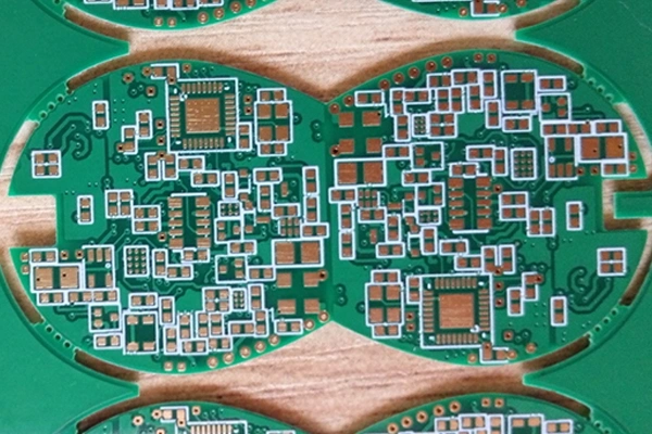
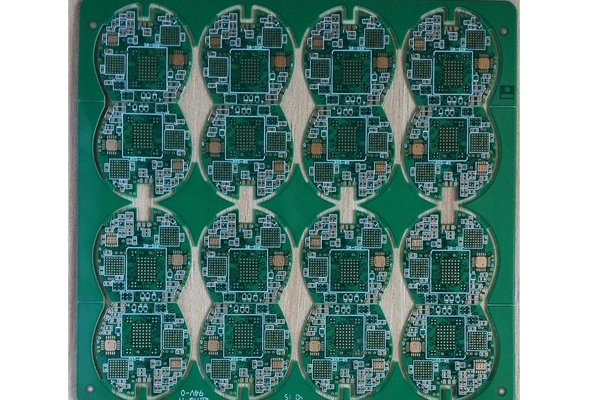
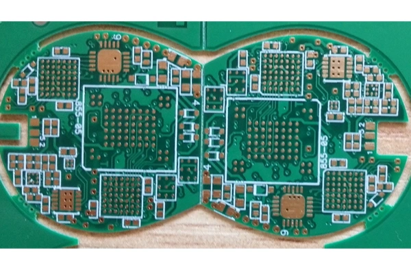
Layer count: 6 HDI PCB
Material: FR4 , 0.6mm, high TG, 0.5 OZ for all layer
Minimum track: 3 mil
Minimum space: 3 mil
Minimum hole: 0.15mm
Surface finished: ENIG
Panel size: 220*268mm/16up
Microvia PCBs constitute a core part of today's electronic products, and these help in small size and high output. These multi-layered circuit boards find applications in electronics such as smartphones, medical technology, automotive, and high-speed communication and many more. We are capable of providing full-service package including design, fabrication and assembly as a professional microvia PCB manufacturer.
A microvia PCB is a type of HDI PCB which uses microvias to connect adjacent layers in a circuit board. Microvias are tiny holes, generally with a diameter of 0.006 inches (150 microns) or less that allow for greater wiring density and smaller designs. These circuit boards have small vias, narrow lines and spaces, and high I/O and are granted by complex interconnections attributed to microvia technology in a small space for occlusion.
The production procedure of microvia PCBs is a combination of high-tech products including life science and electronics.
Material Selection Process
The first step in the process is the appropriate material selection with importance given to thin dielectric layers and copper foils which promote high-density circuits of the HDI PCBs. As a professional manufacturer, we select the materials with good thermal and mechanical characteristics for durable and stable microvia PCB.
Laser Drilling
The production of microvias is the most critical process in manufacturing Microvia PCB. Laser drilling enables these holes to be drilled with very high accuracy. This method enables precise interconnections between layers without compromising the integrity of the board.
Plating and Filling
Following drilling, copper is plated in the microvias to create electrical connectivity between layers. Sometimes, the microvias are filled to make up for an uneven surface for to lay down more layers. This step is essential for making sure the PCB is reliable, especially so in demanding HDI applications.
Layer Lamination and Circuit Etching
The pcb layers are the laminated under heat and pressure to consolidate the lamination into a rigid unit. Then more sophisticated etching is carried out to produce the complex circuit patterns needed for high-density designs.
Surface Finishing and Testing
For board protection and better solderability, surface finish such as ENIG (Electroless Nickel Immersion Gold) or OSP (Organic Solderability Preservative) are used. In the end, the PCB is subjected to the testing to ensure it has the desired performance.
As an experienced manufacturer, we integrate state-of-the-art technology with a strong commitment to quality. Our knowledge in HDI technology enables us to produce high precision, high reliability, and high performance PCBs. We realize the complexities of contemporary electronic design and collaborate with our customers to offer solutions tailored to their requirements. Whether you need single-layer, multilayer, or stacked microvia PCBs, our world-class manufacturing facilities and experienced engineering team will ensure the best quality.
Microvia PCBs are needed to make high-performance, densely compact electronics and their production demands knowhow and high accuracy. Selecting the right microvia PCB manufacturer to partner with is the key to success for your project. With our state of the art technology, commitment to quality and years of experience in HDI PCB manufacturing, you will find the perfect partner to turn your designs into reality